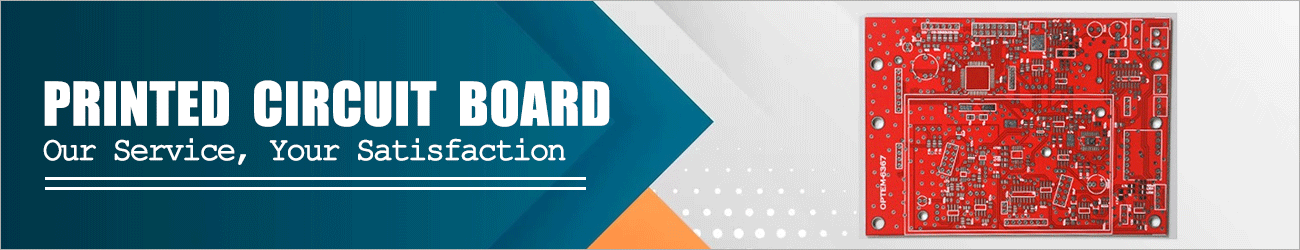
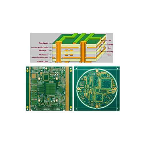
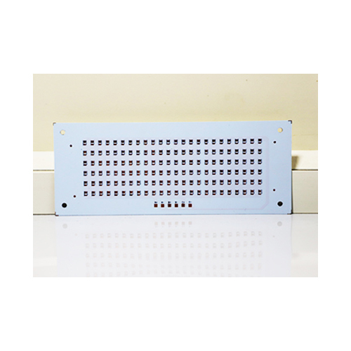
About Multilayer PCB
Select this enlightened Multilayer PCB for your next project and benefit from a potent engineering solution, perfect for demanding telecom, medical, automotive, or industrial control applications. This virtuoso product, with up to 32 layers, supports fine alignment tolerance (50m), a robust aspect ratio (10:1), and accommodates through, blind, and buried vias. Available in multiple vivid colors and panel sizes up to 600mm x 1200mm, it's vacuum sealed for anti-static safety. Customization and potent reliability combine-act now, as our discount offers are ending soon!
Versatile Utility and Exceptional Advantages of Multilayer PCBs
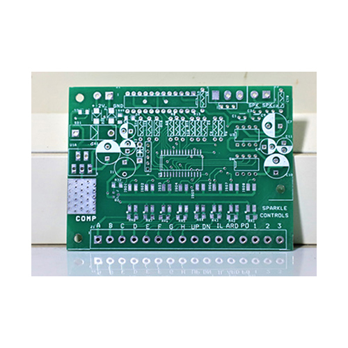
Multilayer PCBs excel across varied use types, from medical instruments to advanced telecom systems. Their potent layered structure ensures signal integrity and compact, enlightened designs for space-saving applications. Easy to integrate, these PCBs require alignment per manufacturer guidelines and are ideal for high-reliability use. Their unique combination of strength and flexibility gives users a competitive advantage in demanding operational environments.
Payment Flexibility and Secure Handover of Multilayer PCBs
Payment terms are designed for your convenience, including industry-standard options. FOB port is typically in India, ensuring streamlined global logistics. We provide sample units for verification before order finalization. Upon confirmation, each PCB is securely packed in vacuum sealed anti-static packaging and prepared for dispatch, ensuring the product is shipped safely and handed over to your preferred logistics provider for fast delivery.
FAQ's of Multilayer PCB:
Q: How do I select the optimal Multilayer PCB configuration for my application?
A: Assess your application's requirements for layer count, aspect ratio, copper thickness, operating temperature, and board size. Our technical team can help guide you to the right selection for telecom, medical, automotive, or industrial control settings.
Q: What testing processes are used to ensure PCB quality?
A: All Multilayer PCBs undergo rigorous Flying Probe and E-test examinations to guarantee performance, signal integrity, and insulation resistance prior to shipment.
Q: When can I expect my Multilayer PCB to be dispatched after order confirmation?
A: Once your order and payment are confirmed, production starts promptly. Standard packing and dispatch are completed swiftly, with lead times depending on your specific requirements and order volume.
Q: Where do you ship from, and what packaging is used?
A: We ship from India, utilizing vacuum-sealed anti-static packaging to protect each PCB during transportation and handling.
Q: What are the main benefits of using these Multilayer PCBs in my project?
A: Benefits include efficient space usage, reliable electrical performance, advanced customization, superior temperature resistance, and compliance with stringent flame resistance and voltage endurance standards.


 Send Inquiry

 Send Inquiry
 Send SMS